The full form of MOSFET is “Metal Oxide Semiconductor Field Effect Transistor”. Now here we are going to discuss MOSFET and its types. Also, I will discuss the basic construction of MOSFET. We know a lot many transistors but this transistor was designed by Martin M. Atalla and Dawon Kahng in 1959 at Bell Labs.
Types of MOSFETs:
- Depletion Type MOSFET
- Enhancement Type MOSFET
Here in this article, we are going to discuss only Depletion type MOSFET. In the next post, we will discuss enhancement type MOSFET.

Depletion Type Mosfet Construction:
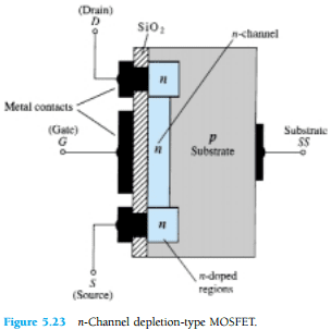
The basic construction of the n-channel depletion type MOSFET is shown in the above figure. A slab of p-type material is formed from a silicon base and is referred to as the substrate. It is the foundation upon which the device will be constructed. In some cases, the substrate is internally connected to the source terminal. However, many discrete devices provide an additional terminal labelled SS, resulting in a four-terminal device, such as that appearing in the figure shown above.
The source and drain terminals are connected through metallic contacts to n-doped regions linked by an n-channel as shown in the figure. The gate is also connected to a metal contact surface but remains insulated from the n-channel by a very thin silicon dioxide (SiO2) layer. SiO2 is a particular type of insulator referred to as a dielectric that sets up opposing electric fields within the dielectric when exposed to an externally applied field. The fact that the SiO2 layer is an insulating layer reveals the following fact:
There is no direct electrical connection between the gate terminal and the channel of a MOSFET.
It is the insulating layer of SiO2 in the MOSFET construction that accounts for the very desirable high input impedance of the device. In fact, the input resistance of a MOSFET is often that of the typical JFET, even though the input impedance of most JFETs is sufficiently high for most applications. The very high input impedance continues to fully support the fact that the gate current (IG) is essentially zero amperes for dc biased configurations.
The reason for the label metal-oxide-semiconductor FET is now fairly obvious: metal for the drain, source, and gate connections to the proper surface in particular, the gate terminal and the control to be offered by the surface area of the contact, the oxide for the silicon dioxide insulating layer, and the semiconductor for the basic structure on which the n-type and p-type regions are diffused. The insulating layer between the gate and channel has resulted in another name for the device: insulated gate FET or IGFET, although this label is used less and less in current literature.
Depletion Type MOSFET Working Principle:
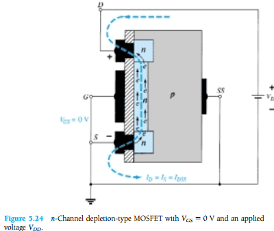
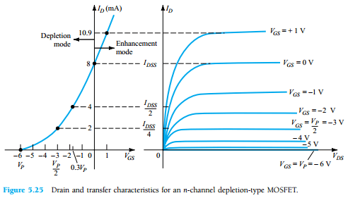
In figure 5.24 the gate-to-source voltage is set to zero volts by the direct connection from one terminal to the other and a voltage VDS is applied across the drain to source terminals. The result is an attraction for the positive potential at the drain by the free electrons of the n-channel and a current similar to that established through the channel of the JFET. In fact, the resulting current with VGS = 0 V continues to be labelled IDSS, as shown in the characteristics of depletion type MOSFET figure.
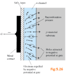
In figure 5.26, VGS has been set at a negative voltage such as 1 V. The negative potential at the gate will tend to pressure electrons toward the p-type substrate (like charges repel) and attract holes from the p-type substrate (opposite charges attract) as shown in figure 5.26.
Depending on the magnitude of the negative bias established by VGS, a level of recombination between electrons and holes will occur that will reduce the number of free electrons in the n-channel available for conduction. The more negative the bias, the higher the rate of recombination.
The resulting level of drain current is therefore reduced with increasing negative bias for VGS as shown in the figure below for VGS = – 1 V, – 2 V, and so on, to the pinch-off level of 6 V., The resulting levels of drain current and the plotting of the transfer curve proceeds exactly as described for the JFET.
For positive values of VGS, the positive gate will draw additional electrons (free carriers) from the p-type substrate due to the reverse leakage current and establish new carriers through the collisions resulting from accelerating particles. As the gate-to-source voltage continues to increase in the positive direction, characteristics of depletion-type MOSFET reveal that the drain current will increase at a rapid rate for the reasons listed above.
The vertical spacing between the VGS = 0 V and VGS = 1 V curves of Fig. 5.25 is a clear indication of how much the current has increased for the 1-V change in VGS. Due to the rapid rise, the user must be aware of the maximum drain current rating since it could be exceeded with a positive gate voltage.
That is, for the device in the figure showing characteristics of depletion type MOSFET, the application of a voltage VGS = 4 V would result in a drain current of 22.2 mA, which could possibly exceed the maximum rating (current or power) for the device.
As revealed above, the application of a positive gate-to-source voltage has “enhanced” the level of free carriers in the channel compared to that encountered with VGS = 0 V.For this reason the region of positive gate voltages on the drain or transfer characteristics is often referred to as the enhancement region, with the area between cutoff and the saturation level of IDSS referred to as the depletion region.
It is exciting and helpful that Shockley’s equation will continue to be applicable for the depletion-type MOSFET characteristics in both the depletion and enhancement regions. For both regions, it is simply necessary that the proper sign be included with VGS in the equation and the sign is carefully monitored in the mathematical operations.
Conclusion:
Now here we have discussed depletion-type MOSFET construction & working & its characteristics.
Comment below for any Queries.