Common Emitter Configuration:
The most frequently encountered transistor configuration appears in Fig. for the PNP and NPN transistors. It is called the common emitter configuration since the emitter is common or reference to both the input and output terminals (in this case common to both the base and collector terminals). Two sets of characteristics are again necessary to describe fully the behaviour of the common emitter configuration one for the input or base-emitter circuit and one for the output or collector-emitter circuit.Both are shown in the figure.
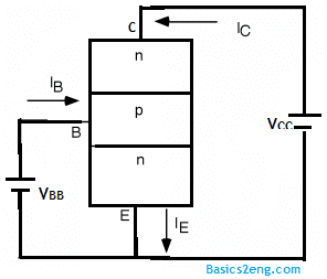
The emitter, collector, and base currents are shown in their actual conventional current direction.Even though the transistor configuration has changed, the current relations developed earlier for the common base configuration are still applicable.That is,
IE = IC + IB and IC = α IE
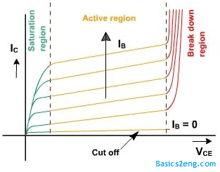
For the common emitter configuration the output characteristics are a plot of the output current (IC) versus output voltage (VCE) for a range of values of input current (IB).The input characteristics are a plot of the input current (IB) versus the input voltage (VBE) for a range of values of output voltage (VCE).
Common Emitter Configuration Characteristics:
Note that on the characteristics of common emitter configuration the magnitude of IB is in microamperes, compared to milliamperes of IC. Consider also that the curves of IB are not as horizontal as those obtained for IE in the common-base configuration, indicating that the collector-to-emitter voltage will influence the magnitude of the collector current.
The active region for the common emitter configuration is that portion of the upper-right quadrant that has the greatest linearity, that is, that region in which the curves for IB are nearly straight and equally spaced. In Fig. shown this region exists to the right of the vertical dashed line at VCE(sat) and above the curve for IB equal to zero.The region to the left of VCE(sat) is called the saturation region.
In the active region of a common emitter amplifier the collector-base junction is reverse-biased, while the base-emitter junction is forward-biased.
You will recall that these were the same conditions that existed in the active region of the common base configuration.The active region of the common emitter configuration can be employed for voltage, current, or power amplification.The cutoff region for the common emitter configuration is not as well defined as for the common base configuration.
Note on the collector characteristics of the figure that IC is not equal to zero when IB is zero. For the common base configuration, when the input current IE was equal to zero, the collector current was equal only to the reverse saturation current ICO, so that the curve IE = 0 and the voltage axis were, for all practical purposes, one.