Common Base Configuration:
The notation and symbols used in conjunction with the transistor in the majority of texts and manuals published today are indicated in the figure for the common base configuration with PNP and NPN transistors.The common-base terminology is derived from the fact that the base is common to both the input and output sides of the configuration.
In addition, the base is usually the terminal closest to, or at, ground potential.Throughout this book, all current directions will refer to conventional (hole) flow rather than electron flow.This choice was based primarily on the fact that the vast amount of literature available at educational and industrial institutions employs conventional flow and the arrows in all electronic symbols have a direction defined by this convention.Recall that the arrow in the diode symbol defined the direction of conduction for conventional current. For the transistor:
The arrow in the graphic symbol defines the direction of emitter current (conventional flow) through the device.
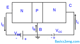
All the current directions appearing in Fig. are the actual directions as defined by the choice of conventional flow. Note in each case that IE =IC+IB. Note also that the applied biasing (voltage sources) are such as to establish a current in the direction indicated by each branch. That is, compare the direction of IE to the polarity or VEE for each configuration and the direction of IC to the polarity of VCC.
To fully describe the behaviour of a three-terminal device such as the common base amplifiers of the figure requires two sets of characteristics – one for the driving point or input parameters and the other for the output side. The input set for the common-base amplifier as shown in figure will relate an input current (IE) to an input voltage (VBE) for various levels of the output voltage (VCB).
The output set will relate an output current (IC) to an output voltage (VCB) for various levels of input current (IE) as shown in the below figure.The output or collector set of characteristics has three basic regions of interest, as indicated in the figure the active, cutoff, and saturation regions.The active region is the region normally employed for linear (undistorted) amplifiers. In particular:
In the active region, the collector-base junction is reverse-biased, while the base-emitter junction is forward-biased.
Common Base Configuration Characteristics:
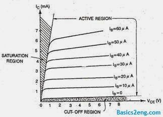
The active region is defined by the biasing arrangements of above figure.The above figure shows characteristics of Common Base Configuration.At the lower end of the active region, the emitter current (IE) is zero, the collector current is simply that due to the reverse saturation current ICO, as indicated in the above figure. The current ICO is so small (micro amperes) in magnitude compared to the vertical scale of IC (milliamperes) that it appears on virtually the same horizontal line as IC=0. The circuit conditions that exist when IE=0 for the common base configuration is shown in the above figure.The notation most frequently used for ICO on data and specification sheets is, as indicated in Fig., ICBO. Because of improved construction techniques, the level of ICBO for general-purpose transistors (especially silicon) in the low- and mid power ranges is usually so low that its effect can be ignored. However, for higher power units ICBO will still appear in the microampere range. In addition, keep in mind that ICBO, like Is, for the diode (both reverse leakage currents) is temperature sensitive. At higher temperatures, the effect of ICBO may become an important factor since it increases so rapidly with temperature.Note in figure that as the emitter current increases above zero, the collector current increases to a magnitude essentially equal to that of the emitter current as determined by the basic transistor-current relations. Note also the almost negligible effect of VCB on the collector current for the active region. The curves clearly indicate that a first approximation to the relationship between IE and IC in the active region is given by
IC = IE
As inferred by its name, the cutoff region is defined as that region where the collector current is 0 A, as revealed in the above figure.In addition:
In the cutoff region, the collector-base and base-emitter junctions of a transistor are both reverse-biased.
The saturation region is defined as that region of the characteristics to the left of VCB=0 V. The horizontal scale in this region was expanded to clearly show the dramatic change in characteristics in this region. Note the exponential increase in collector current as the voltage VCB increases toward 0 V.
In the saturation region, the collector-base and base-emitter junctions are forward-biased.
The input characteristics from the above figure reveal that for fixed values of collector voltage (VCB), as the base-to-emitter voltage increases, the emitter current increases in a manner that closely resembles the diode characteristics. In fact, increasing levels of VCB have such a small effect on the characteristics that as a first approximation the change due to changes in VCB can be ignored and the characteristics are drawn as shown in the above figure.If we then apply the piecewise-linear approach, the characteristics of the figure will result.Taking it a step further and ignoring the slope of the curve and therefore the resistance associated with the forward-biased junction will result in the characteristics of Common Base Configuration in the above figure.For the analysis to follow in this book the equivalent model of the figure will be employed for all dc analysis of transistor networks.That is, once a transistor is in the “on” state, the base-to-emitter voltage will be assumed to be the following
VBE = 0.7 V
In other words, the effect of variations due to VCB and the slope of the input characteristics will be ignored as we strive to analyse transistor networks in a manner that will provide a good approximation to the actual response without getting too involved with parameter variations of less importance.It is important to fully appreciate the statement made by the characteristics of the figure.They specify that with the transistor in the “on” or active state the voltage from base to emitter will be 0.7 V at any level of emitter current as controlled by the external network.In fact, at the first encounter of any transistor configuration in the dc mode, one can now immediately specify that the voltage from base to emitter is 0.7 V if the device is in the active region a very important conclusion for the dc analysis to follow.