Tunnel diode Construction:
Now here we are going to discuss construction and working principle of Tunnel diode.This diode has two terminals.This tunnel diode is also known as Esaki diode.Here is the symbol of tunnel diode or Esaki diode.

Definition of tunnel diode is :: The Tunnel or Esaki diode is a junction diode which exhibits negative resistance under low forward bias conditions. An ordinary PN junction diode has an impurity concentration of about 1 part in 10pow(8) with this amount of doping the width of the depletion layer is of an order of 5 microns.This potential barrier restrains the flow of carriers from majority carrier side to the minority carrier side.If the concentration of impurity atoms is greatly increased to the level of 1 part in 10pow(3),the device characteristics are completely changed.The width of the junction barrier varies inversely as the square root of the impurity concentration and therefore ,is reduced from 5 micron to less than 100 Armstrongs.This thickness is about 1/50th of the wavelength of visible light.for such thin potential energy barriers ,the electrons will penetrate through the junction rather than surmounting them.This quantum mechanical behaviour is referred to as tunnelling and hence, these high-impurity-density PN junction devices are called tunnel diodes.
Must Read:
Tunnel diode Characteristics:
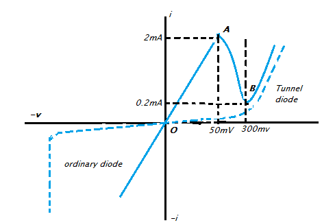
The V-I characteristic for a typical germanium tunnel diode is shown below.It is seen that at first current rises sharply as applied voltage is increased ,where it would have risen slowly for an ordinary PN junction diode(shown by dashed line).Also ,the reverse current is much larger for comparable back bias than in other diodes due to the thinness of the junction.The interesting portion of the characteristics starts at point A on the curve i.e. peak voltage.As the forward bias is increased beyond this point,the forward current drops and continues to drop until point B is reached.This is valley voltage.At B,the current starts to increase once again and does so very rapidly as bias is increased further.Beyond this point, characteristic resembles that of an ordinary diode.apart from peak voltage and valley voltage,the other two parameters normally used to specify the diode behaviour are at the peak current and the peak-to-valley current ratio,which are 2mA and 10nA respectively , as shown.
The V-I characteristics of the tunnel diode illustrate that it exhibits dynamic resistance between A and B.Below figure shows energy level diagrams of the tunnel diode for three bias levels.The shaded areas show the energy states occupied by electrons in the valence band,whereas the cross-hatched regions represent energy states in the conduction band occupied by the electrons.The levels of which the energy states are occupied by electrons on either side of the junctions are shown by dotted lines.When the bias is zero,these lines are at the same height.Unless energy is imparted to the electrons from some external source,the energy possessed by the electrons on the N-side of the junction is insufficient to permit them to climb over the junction barrier to reach the P-side.However ,quantum mechanics show that there is a finite probability for the electrons to tunnel through the junction to reach the other side,provided there are allowed empty states in the P-side of the junction at the same energy level.Hence the forward current is zero.
Tunnel diode Operation:
When the small forward bias is applied to the junction,the energy level of the p-side is lower as compared with the N-side.As shown in figure 3 ,electrons in the conduction band of the N-side see empty energy level on the P-side.Hence ,tunnelling from N-side to P-side takes place.Tunnelling on other directions is not possible because the valence band electrons on the P-side are now opposite to the forbidden gap in the N-side.
When the forward bias is raised beyond this point,tunnelling decreases as shown in the above figure.The energy of P-side is now decreased further , with the result that fewer conduction band electrons on the N-side are opposite to the unoccupied P-side energy levels.As the bias is raised,forward current drops.This corresponds to the negative resistance region of the diode characteristic.As the forward bias is raised still further,tunnelling stops altogether and it behaves as a normal PN junction diode.
Now here as we discussed the entire concept of tunnel diode operation and its characteristics.You can also print this article pdf .If you have any doubts regarding this article you can mail us as palakalaamarnath@gmail.com
If you want to get more information, schematics, structures, definition etc about Tunnel Diode , visit our site:
http://911electronic.com/
Thank you for your comment and for sharing the link to your website. I will definitely check it out for more information about tunnel diodes. It’s always helpful to have additional resources to refer to when learning about a new topic.