Schottky Barrier Diode – Operation:
Schottky barrier diode is an extension of the oldest semiconductor device that is the point contact diode.Here, the metal-semiconductor interface is a surface, Schottky barrier rather than a point contact.The Schottky diode is formed when a metal, such as Aluminium, is brought into contact with a moderately doped N-type semiconductor as shown in the below figure.It is a unipolar device because it has electrons as majority carriers on both sides of the junction.
Hence, there is no depletion layer formed near the junction.It shares the advantage of point contact diode in that there is no significant current from the metal to the semiconductor with reverse bias.Thus, the delay present in the junction diodes due to hole-electron recombination time is absent here.Hence, because of the large contact area between the metal and semiconductor than in the point contact diode, the forward resistance is lower and so is noise.
![]()
Schottky barrier diode Construction:
A metal–semiconductor junction is formed between a metal and a
semiconductor, creating a Schottky barrier (instead of a semiconductor – semiconductor junction as in conventional diodes).Typical metals used are molybdenum, platinum, chromium or tungsten, and certain silicides, e.g. palladium silicide and platinum silicide; andthe semiconductor would typically be n-type silicon.
The metal side acts as the anode and n-type semiconductor acts as the cathode of the diode.This Schottky barrier results in both very fast switching and low forward voltage drop.The choice of the combination of the metal and semiconductor determines the forward voltage of the diode.
Both N-type and P-type semiconductors can develop Schottky barriers; the p-type typically has a much lower forward voltage.As the reverse leakage current increases dramatically with lowering the forward voltage, it can not be too low; the usually employed range is about 0.5-0.7 V and p-type semiconductors are employed only rarely.
Titanium silicide and other refractory silicides, which are able to withstand the temperatures needed for source/drain annealing in CMOS processes, usually have too low forward voltage to be useful; processes using these silicides therefore usually do not offer Schottky diodes.With increased doping level of the semiconductor the width of the depletion region drops.
Below certain width, the charge carriers can tunnel through the depletion region.At very high doping levels the junction does not behave as a rectifier anymore and becomes an ohmic contact.This can be used for simultaneous formation of ohmic contacts and diodes, as diodes form between the silicide and lightly doped n-type region and ohmic contacts form between the silicide and a heavily doped n-type or p-type region.
Lightly doped P regions pose a problem as the resulting contact has too high resistance for a good ohmic contact and too low forward voltage and too high reverse leakage to be a good diode.As the edges of the Schottky contact are fairly sharp, high electric field gradient occurs around them which limits the reverse breakdown voltage.
Various strategies are used, from guard rings to overlaps of metallization to spread out the field gradient.The guard rings consume valuable die area and are used primarily for large higher-voltage diodes, while overlapping metallization is employed primarily with smaller, low-voltage diodes.Schottky diodes are often used as anti-saturation clamps on transistors (a Schottky transistor).
Palladium silicide ones are excellent here due to their lower forward voltage (which has to be lower than the forward voltage of the base-collector junction); platinum silicide ones have forward voltage closer to that and require more attention in layout.The Schottky temperature coefficient is lower than the coefficient of the B-C junction, which limits the use of PtSi at higher temperatures.For power schottky diodes the parasitic resistances of the buried N+ layer and the epitaxial n-type layer become important.
The resistance of the epitaxial layer is more important here than for a transistor as the current has to cross its entire thickness. It however serves as a distributed ballasting resistor over the entire area of the junction and prevents localized thermal runaway under usual conditions.In comparison with the power p–n diodes the Schottky diodes are less rugged.
The junction lies in direct contact to the thermally sensitive metallization, a Schottky diode can therefore dissipate less power than an equivalent-size p–n one with deep-buried junction, before failing – especially during reverse breakdown. The relative advantage of lower forward voltage of Schottky diodes is diminished at higher forward currents, where the voltage drop is dominated by the series resistance.
The forward current is dominated by electron flow from semiconductor to metal and the reverse is mainly due to electron from metal to semiconductor.As there is very little minority carrier injection from semiconductor into metal, Schottky diodes are also said to be majority carrier devices.The diode is also reffered to as hot carrier diode because when it is forward biased, conduction of electrons on the N-side gains sufficient energy to cross the junction and enter the metal.Since these electrons plunge into the metal with large energy, they are commonly called as hot carriers.
Schottky barrier diode – Characteristics:
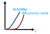
Above figure shows the V-I characteristics of a Schottky and a PN junction diode. The current in a PN junction diode is controlled by the diffusion of minority carriers whereas the current in the schottky diode results from the flow of majority carriers over the potential barrier at the metal-semiconductor junction.The reverse saturation current for a Schottky diode is larger than that of a PN junction diode.The storage time for a Schottky diode is theoretically zero.The schottky diode has a smaller turn-on voltage and shorter switching time than the PN junction diode.
Schottky barrier diode Applications:
- Schottky diode can be used for rectification of signals of frequencies even exceeding 300 MHz.
- It is commonly used in switching power supplies at frequencies of 20 GHz.
- Its low noise figure finds application in sensitive communication receivers like radars.
- It is also used in clipping and clamping circuits and in computer gating.
Must Read: