We have already discussed that two types of MOSFET‘s are there .In the previous post we have discussed about Depletion type MOSFET .Now here we are discuss about Enhancement type MOSFET .We will know how its construction is and its working principle.
“MOSFET = Metal Oxide Semiconductor Field Effect Transistor”
Construction of Enhancement type MOSFET:
The basic construction of the n-channel enhancement-type MOSFET is provided in Fig. 5.31.A slab of p-type material is formed from a silicon base and is again referred to as the substrate. As with the depletion-type MOSFET, the substrate is sometimes internally connected to the source terminal, while in other cases a fourth lead is made available for external control of its potential level. The source and drain terminals are again connected through metallic contacts to n-doped regions, but note in Fig.5.31 the absence of a channel between the two n-doped regions.This is the primary difference between the construction of depletion type MOSFET and enhancement type MOSFET—the absence of a channel as a constructed component of the device.
———————————————————————————————–
If you are an electrical engineering student don’t forget to Read below:
- Measurement of high resistance by Mega Ohm bridge method
- Construction and Working principle of Depletion type MOSFET
- Construction of Megger test used for measuring Insulation resistance
Like and Follow Us At Facebook , Google+ , Twitter .
———————————————————————————————–
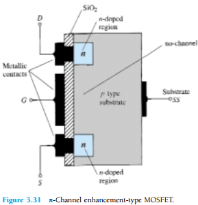
The SiO2 layer is still present to isolate the gate metallic platform from the region between the drain and source, but now it is simply separated from a section of the p-type material. In summary, therefore, the construction of an enhancement-type MOSFET is quite similar to that of the depletion-type MOSFET, except for the absence of a channel between the drain and source terminals.
Operation of Enhancement type MOSFET:
If VGS is set at 0 V and a voltage applied between the drain and source of the device of Fig. 5.31, the absence of an n-channel (with its generous number of free carriers) will result in a current of effectively zero amperes—quite different from the depletion-type MOSFET and JFET where ID = IDSS.It is not sufficient to have a large accumulation of carriers (electrons) at the drain and source (due to the n-doped regions) if a path fails to exist between the two. With VDS some positive voltage, VGS at 0 V,and terminal SS directly connected to the source, there are in fact two reverse-biased p-n junctions between the n-doped regions and the p-substrate to oppose any significant flow between drain and source.In Fig. 5.32 both VDS and VGS have been set at some positive voltage greater than 0 V, establishing the drain and gate at a positive potential with respect to the source. The positive potential at the gate will pressure the holes (since like charges repel) in the p-substrate along the edge of the SiO2 layer to leave the area and enter deeper regions of the p-substrate, as shown in the figure.
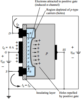
The result is a depletion region near the SiO2 insulating layer void of holes. However, the electrons in the p-substrate (the minority carriers of the material) will be attracted to the positive gate and accumulate in the region near the surface of the SiO2 layer. The SiO2 ayer and its insulating qualities will prevent the negative carriers from being absorbed at the gate terminal. As VGS increases in magnitude, the concentration of electrons near the SiO2 surface increases until eventually the induced n-type region can support a measurable flow between drain and source. The level of VGS that results in the significant increase in drain current is called the threshold voltage and is given the symbol VT. On specification sheets it is referred to as VGS(Th) , although VT is less unwieldy and will be used in the analysis to follow. Since the channel is nonexistent with VGS = 0 V and “enhanced” by the application of a positive gate-to-source voltage, this type of MOSFET is called an enhancement-type MOSFET. Both depletion type MOSFET and enhancement type MOSFET have enhancement-type regions, but the label was applied to the latter since it is its only mode of operation.
As VGS is increased beyond the threshold level, the density of free carriers in the induced channel will increase, resulting in an increased level of drain current. However, if we hold VGS constant and increase the level of VDS , the drain current will eventually reach a saturation level as occurred for the JFET and depletion-type MOSFET. The leveling off of ID is due to a pinching-off process depicted by the narrower channel at the drain end of the induced channel as shown in Fig. 5.33. Applying Kirchhoff’s voltage law to the terminal voltages of the MOSFET of Fig. 5.33, we find that
![]()
If VGS is held fixed at some value such as 8 V and VDS is increased from 2 to 5 V, the voltage VDG [by Eq. (5.11)] will drop from 6 to 3 V and the gate will become less and less positive with respect to the drain. This reduction in gate-to-drain voltage will in turn reduce the attractive forces for free carriers (electrons) in this region of the induced channel, causing a reduction in the effective channel width.
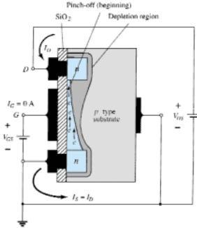
Eventually, the channel will be reduced to the point of pinch-off and a saturation condition will be established as described earlier for the JFET and depletion-type MOSFET.In other words, any further increase in VDS at the fixed value of VGS will not affect the saturation level of ID until breakdown conditions are encountered.The drain characteristics of enhancement type MOSFET in Fig. 5.34 reveal that for the device of Fig. 5.33 with VGS = 8 V, saturation occurred at a level of VDS = 6 V. In fact, the saturation level for VDS is related to the level of applied VGS by
![]()
Obviously, therefore, for a fixed value of VT, then the higher the level of VGS, the more the saturation level for VDS, as shown in Fig. 5.33 by the locus of saturation levels.
Characteristics of Enhancement type MOSFET :
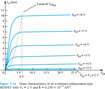
For the characteristics of Fig. 5.33 the level of VT is 2 V, as revealed by the fact that the drain current has dropped to 0 mA. In general, therefore:For values of VGS less than the threshold level, the drain current of an enhancement-type MOSFET is 0 mA.Figure 5.34 clearly reveals that as the level of VGS increased from VT to 8 V, the resulting saturation level for ID also increased from a level of 0 to 10 mA. In addition, it is quite noticeable that the spacing between the levels of VGS increased as the magnitude of VGS increased, resulting in ever-increasing increments in drain current.For levels of VGS = VT, the drain current is related to the applied gate-to-source voltage by the following nonlinear relationship:
Again, it is the squared term that results in the nonlinear (curved) relationship between ID and VGS .The k term is a constant that is a function of the construction of the device. The value of k can be determined from the following equation [derived from Eq. (5.13)] where ID(on) and VGS(on) are the values for each at a particular point on the characteristics of the device.
![]()
Conclusion:
Now here we have discussed the entire concept of Enhancement type MOSFET and its characteristics.
Comment below for any Queries.