Unijunction Transistor (UJT):
A unijunction transistor (abbreviated as UJT) is a three-terminal semiconductor switching device.This device has a unique characteristic that when it is triggered, the emitter current increases regeneratively until it is limited by emitter power supply.Due to this characteristic, the unijunction transistor can be employed in a variety of applications e.g., switching, pulse generator, saw-tooth generator etc.
Unijunction Transistor Construction:
The figure(i) below shows the basic structure of a unijunction transistor.It consists of an n-type silicon bar with an electrical connection on each end.The leads to these connections are called base leads base-one B1 and base two B2.Part way along the bar between the two bases, nearer to B2 than B1, a PN junction is formed between a p-type emitter and the bar.The lead to this junction is called the emitter lead E.The figure(ii) below shows the symbol of unijunction transistor.
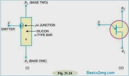
Note that emitter is shown closer to B2 than B1.The following points are worth noting:
(i) Since the device has one PN junction and three leads, it is commonly called a unijunction transistor (uni means single).
(ii) With only one PN junction, a device is really a form of a diode. Because the two base terminals are taken from one section of the diode, this device is also called double-based diode.
(iii) The emitter is heavily doped having many holes. The n region, however, is lightly doped.For this reason, the resistance between the base terminals is very high ( 5 to 10 kΩ) when emitter lead is open.
Unijunction Transistor Operation:
The figure below shows the basic circuit operation of a unijunction transistor.The device has normally B2 positive w.r.t. B1.
(i) If voltage VBB is applied between B2 and B1 with emitter open, a voltage gradient is established along the n-type bar.Since the emitter is located nearer to B2, more than half of VBB appears between the emitter and B1.The voltage V1 between emitter and B1 establishes a reverse bias on the PN junction and the emitter current is cut off. Of course, a small leakage current flows from B2 to emitter due to minority carriers.
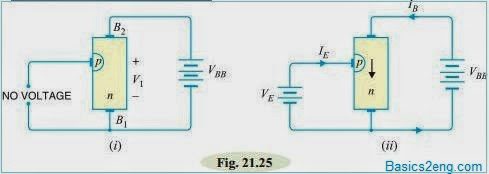
(ii) If a positive voltage is applied at the emitter [See the above figure(ii)], the pn junction will remain reverse biased so long as the input voltage is less than V1.If the input voltage to the emitter exceeds V1, the pn junction becomes forward biased.Under these conditions, holes are injected from p-type material into the n-type bar.These holes are repelled by positive B2 terminal and they are attracted towards B1 terminal of the bar.This accumulation of holes in the emitter to B1 region results in the decrease of resistance in this section of the bar.
The result is that internal voltage drop from emitter to B1 is decreased and hence the emitter current IE increases.As more holes are injected, a condition of saturation will eventually be reached. At this point, the emitter current is limited by emitter power supply only.The device is now in the ON state.
(iii) If a negative pulse is applied to the emitter, the pn junction is reverse biased and the emitter current is cut off. The device is then said to be in the OFF state.
Unijunction Transistor(UJT) Equivalent Circuit:
The figure below shows the equivalent circuit of Unijunction Transistor (UJT).The resistance of the silicon bar is called the interbase resistance RBB.The inter-base resistance is represented by two resistors in series viz.
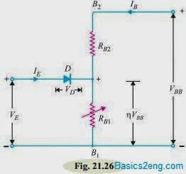
(a) RB2 is the resistance of silicon bar between B2 and the point at which the emitter junction lies.
(b) RB1 is the resistance of the bar between B1 and emitter junction. This resistance is shown variable because its value depends upon the bias voltage across the pn junction.The pn junction is represented in the emitter by a diode D.The circuit action of a UJT can be explained more clearly from its equivalent circuit.
(i) With no voltage applied to the UJT, the inter-base resistance is given by ;
RBB = RB1 + RB2
The value of RBB generally lies between 4 kΩ and 10 kΩ.
(ii) If a voltage VBB is applied between the bases with emitter open, the voltage will divide up across RB1 and RB2.
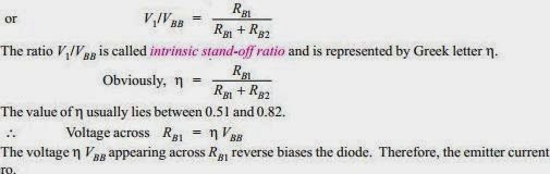
Voltage across RB1, V1 = {RB1/[RB1 + RB2]}*VBB
is zero.
(iii) If now a progressively rising positive voltage is applied to the emitter, the diode will become forward biased when input voltage exceeds η VBB
by VD, the forward voltage drop across the silicon diode i.e.
VP = η VBB + VD
where VP = ‘peak point voltage’
VD = forward voltage drop across silicon diode (j0.7 V)
When the diode D starts conducting, holes are injected from p-type material to the n-type bar.These holes are swept down towards the terminal B1.This decreases the resistance between emitter and B1 (indicated by variable resistance symbol for RB1)and hence the internal drop from emitter to B1.The emitter current now increases regeneratively until it is limited by the emitter power supply.
Unijunction Transistor(UJT) Characteristics:
The figure below shows the curve between emitter voltage (VE) and emitter current (IE) of a UJT at a given voltage VBB between the bases.This is known as the emitter characteristic of UJT.The following points may be noted from the characteristics :
(i) Initially, in the cut-off region, as VE increases from zero, slight leakage current flows from terminal B2 to the emitter.This current is due to the minority carriers in the reverse biased diode.
(ii) Above a certain value of VE, forward IE begins to flow, increasing until the peak voltage VP and current IP are reached at point P.
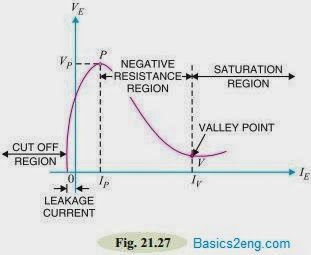
(iii) After the peak point P, an attempt to increase VE is followed by a sudden increase in emitter current IE with a corresponding decrease in VE.This is a negative resistance portion of the curve because, with the increase in IE, VE decreases.The device, therefore, has a negative resistance region which is stable enough to be used with a great deal of reliability in many areas e.g., trigger circuits, sawtooth generators, timing circuits.
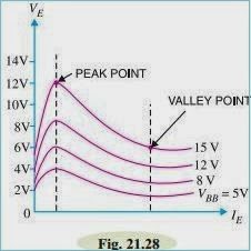
(iv) The negative portion of the curve lasts until the valley point V is reached with valley-point voltage VV and valley-point current IV.After the valley point, the device is driven to saturation.The below figure shows the typical family of VE/ IE characteristics of a UJT at different voltages between the bases.
It is clear that peak-point voltage (= ηVBB + VD) falls steadily with reducing VBB and so does the valley point voltage VV.The difference VP – VV is a measure of the switching efficiency of UJT and can be seen to fall off as VBB decreases.For a general purpose UJT, the peak – point current is of the order of 1 μA at VBB = 20 V with a valley-point voltage of about 2.5 V at 6 mA.
Advantages of UJT:
The UJT was introduced in 1948 but did not become commercially available until 1952. Since then, the device has achieved great popularity due to the following reasons :
(i) It is a low cost device.
(ii) It has excellent characteristics.
(iii) It is a low-power absorbing device under normal operating conditions.
Due to above reasons, this device is being used in a variety of applications.A few include oscillators, trigger circuits, saw-tooth generators, bistable network etc.
Applications of UJT:
Unijunction transistors are used extensively in oscillator, pulse and voltage sensing circuits.Some of the important applications of UJT are discussed below :
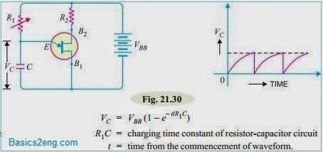
(i) UJT relaxation oscillator: The below figure shows UJT relaxation oscillator where the discharging of a capacitor through UJT can develop a saw-tooth output as shown.When battery VBB is turned on, the capacitor C charges through resistor R1.During the charging period, the voltage across the capacitor rises in an exponential manner until it reaches the peak – point voltage.
At this instant of time, the UJT switches to its low resistance conducting mode and the capacitor is discharged between E and B1.As the capacitor voltage flys back to zero, the emitter ceases to conduct and the UJT is switched off.The next cycle then begins, allowing the capacitor C to charge again.
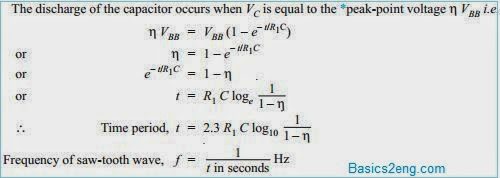
The frequency of the output saw-tooth wave can be varied by changing the value of R1 since this controls the time constant R1C of the capacitor charging circuit.The time period and hence the frequency of the saw-tooth wave can be calculated as follows.Assuming that the capacitor is initially uncharged, the voltage VC across the capacitor prior to breakdown is given by :
(ii) Overvoltage detector:
The figure shows a simple d.c. over-voltage indicator.A warning pilot – lamp L is connected between the emitter and B1 circuit.So long as the input voltage is less than the peak-point voltage (VP) of the UJT, the device remains switched off.However, when the input voltage exceeds VP , the UJT is switched on and the capacitor discharges through the low resistance path between terminals E and B1.The current flowing in the pilot lamp L lights it, thereby indicating the overvoltage in the circuit.